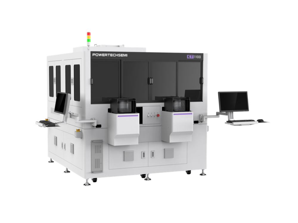
Orientation Inspection Station
Designed and developed based on the needs of the semiconductor industry, using industrial cameras and industrial computers with stable operation, accurate digital transmission, rapid response, clear picture capture, complete and reliable
|
Suspended power supply |
Multiple sites in parallel |
Multi-channel high precision |
Supports multiple extensions |


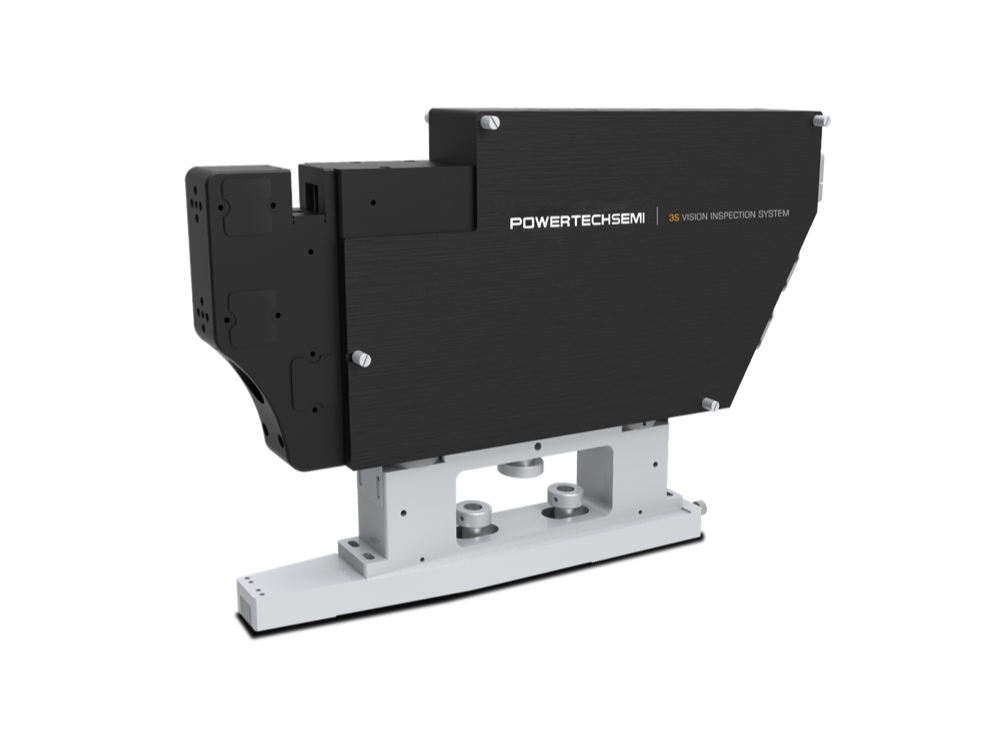
| Type | Direction detection station |
| Description |
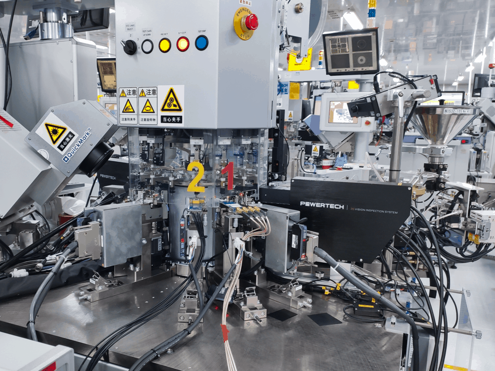
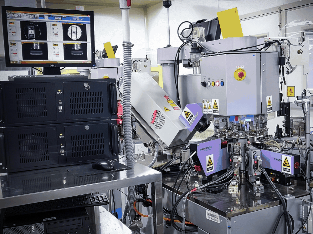
Designed and developed based on the needs of the semiconductor industry, using industrial cameras and industrial computers with stable operation, accurate digital transmission, rapid response, clear picture capture, complete and reliable. It fully meets the production speed of the highest-speed Handler and has complete testing stations to meet various testing needs of customers. QV series inspection system, configurable inspection stations include: 3D inspection station, printing station, taping station, direction station, etc. This system can be used with various Handlers, and the detection range covers various types of semiconductor devices, such as: SOT23, SOD123, SOD323, SOD523, SOD923, SMA, SMB, SMC, SOD882(1006), TO92, TO252, SOD129, MBS, SOP8L and other software The system provides Chinese and English interfaces, multi-level authority control, and a high degree of automation. The software system is 100% linked and developed, and according to the machine vision inspection process, the combination is optimized and easy to operate and apply. All parameters of industrial cameras, such as shutter time, gain, contrast, light source brightness, etc., can be adjusted through software. The QV series machine vision identification system is used for various packaged devices in the semiconductor industry to conduct all-round, high-precision visual inspection of product pins and plastic packages, such as fonts, 2D pins, 3D pins, and plastic package surface defects. Convenient application, simple operation, stable system operation, improving customers' production capacity. Timely detect the accuracy of various devices in the semiconductor industry to improve production efficiency. Perform calibration quickly, ensure zero defective rate, and improve production quality. |
| Function |
• Detect the seal content on the surface of the device (typos, multiple characters, missing characters, defacement, offset, blurred reprint, scratches, cracked plastic package, etc.) • Detect device pin information (direction, foot length, foot width, foot spacing, foot offset, etc.) |
| Basic Configuration |
CCD cameras, industrial lenses, LED light sources, mechanical structural parts |
| SI Detection |
The minimum area is 0.7mm*0.7mm, and the overall average grayscale difference is more than 40 |
| GR&R | <10% |

|
No. 16 Guangming Avenue, New Light Source Industry Base, Nanhai National High tech Zone, Foshan City, Guangdong Province, China |

|
+86 757 83207313 (Sales) |

|
+86 757 83208786 (Sales) |

|
info@powertechsemi.com |


Copyright PowerTECH industrial Co., Ltd. Powertechsmemi.com © 2015 | Privacy policy | Sitmap 粤ICP备17127080号-1